The transistor has several characteristics; one of them is current gain which can be defined as the ratio of output current and input current and is denoted by beta.
Transistor gain or Current gain (β) = load or collector current/ input or base current
Load current = Current gain (beta) × base current
For a normal transistor, beta value is 100.
Above equation tells that the output current is 100 times the input current when beta = 100.
For improved efficiency and high current gain compound devices are used. Darlington pair or Darlington transistor is one of them.
In common emitter configuration of transistor, current gain is the ratio of collector current to base current. We require high gain to drive high loads like an audio amplifier, power regulators, motor controller, etc. A single transistor is not good enough to drive high gain. This problem can be solved by using a Darlington pair.
Basic principle
The transistors are connected in such a way that the input current is first amplified by the first transistor and then to the base of the second transistor. Therefore, the current is again amplified by the second transistor which gives a high current gain at the output.
Circuit operation and design
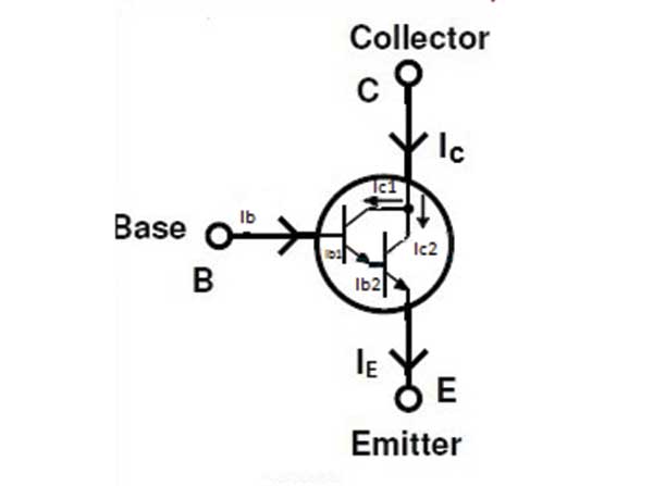
The darlington pair has two transistors connected in a way so that it provides a high value of gain even at low base current. A darlington pair can be formed by two NPN or PNP transistors. Here we will talk about the NPN one.
The transistors used here are in common emitter configuration. One of the transistors is acting like a slave and another one is a master to pull up the gain at the output. The slave transistor or triggering transistor emitter is connected to the base of the master transistor. The slave transistor output emitter current is used for deriving high at base of master transistor. The collector of both the transistors are connected with each other and then with a positive supply like 5V. The current amplified by slave transistor is again amplified by the master transistor. Hence current at emitter is so high which is capable of deriving high loads at the output.
Let’s consider that the current gain of slave transistor is beta1 and the master transistor is beta2. The overall current gain of the transistor will be the product of beta1 and beta2. For a standard transistor beta is 100. Therefore overall current gain is 10000 times of the input current which is very high. So this value of current gain is able to give high current at the output.
Fig. 1: Circuit Diagram of Darlington Pair
Lets say Current gain of the first transistor
The current gain of next transistor,
Beta2 = Ic2 / Ib2
Then Ic2 = Beta2*Ib2
Total current at the collector is Ic = Ic1 + Ic2
Ic= Beta1.Ib1 + Beta2.Ib2
Since the base current of the second transistor is
Ib2 = Beta1.Ib + Ib (since Ib= ib1)
Substituting in the above equationIc = Beta1.
Ib + Beta2.Ib (1+Beta1)
Ic = Ib(Beta1 + Beta2 + Beta1*Beta2)
The individual beta are neglected since the product of both the current gain are very high as compared to their sum. Therefore we can write the above equation as
Ic = Ib (Beta1 +Beta2)
From the above equation, we can analyse the total current gain,
From this derivation, we can see that a small positive voltage at base derives a high current gain. This gain is then used for high current loads
Generally, an NPN silicon type transistor conducts only when its base to emitter junction voltage is greater than or equal to 0.7V (practically, it is 0.65V). But in darlington pair we are using two transistors back to back which increases the value of threshold voltage for both the transistors. Hence for darlington configuration, the base to emitter voltage should be greater than or equal to 1.4V.
Advantages of Darlington Pair
• High current gain than single transistor
• Very High input impedance.
• Easy and convenientYou must be logged in to post a comment.